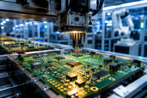
Scaling complex hardware from prototype to volume production fails when high-speed SMT lines lack real-time feedback loops. As components shrink to 0201 passives and 0.35mm pitch BGAs, achieving zero-defect New Product Introduction (NPI) requires replacing traditional visual checks with an integrated 3D inspection stack.
The High-Precision NPI Challenge
Modern power electronics and high-density designs leave no margin for process variance. Traditional NPI workflows rely heavily on post-reflow inspection, where defects like bridging, tombstoning, or head-in-pillow (HiP) are caught only after hundreds of boards have traversed the reflow oven. Reworking fine-pitch micro-BGAs or 01005 passives damages board substrates, compromises thermal integrity, and creates severe NPI delays.
Eliminating rework loops during initial production runs demands catching process deviations at the exact moment they occur.
The 3D Inspection Stack
Achieving zero-defect SMT assembly relies on a continuous, multi-layer 3D inspection stack that validates solder geometry and joint formation across every stage of the line:
- 3D Solder Paste Inspection (SPI): Measures exact solder paste volume, height, and area before component placement. Because roughly 70% of SMT defects originate at the printing stage, 3D SPI prevents solder insufficiency and bridging before expensive silicon meets the board.
- 3D Automated Optical Inspection (AOI): Uses multi-angle volumetric height profiling to verify component alignment, polarity, coplanarity, and lead wetting—eliminating false passes common in standard 2D visual inspection.
- 3D Automated X-Ray Inspection (AXI): Performs non-destructive inline void analysis ($\le 10-15\%$) underneath hidden-lead components like QFNs and BGAs, ensuring full mechanical and thermal pad contact.
Closed-Loop Process Optimization
Data from the inspection stack is only as useful as the line’s ability to act on it. Modern high-precision SMT lines connect 3D SPI and 3D AOI machines directly back to the stencil printer and pick-and-place equipment in a closed feedback loop.
When SPI detects a minor trend in paste offset, it automatically adjusts printer alignment and triggers stencil cleaning cycles before defects occur. Combined with rigorous Front-End Design for Manufacturability (DFM) analysis, closed-loop automation turns NPI from an unpredictable trial-and-error phase into a repeatable science.
At Chipmates.in, we combine closed-loop SMT lines, advanced 3D inspection, and deep DFM engineering to take high-density designs from prototype to zero-defect mass production. Contact us today to review your NPI requirements and optimize your next hardware build.