
Inside the Modern SMT Line: 3D Inspection, Zero-Defect NPI, and the Science of High-Precision Hardware
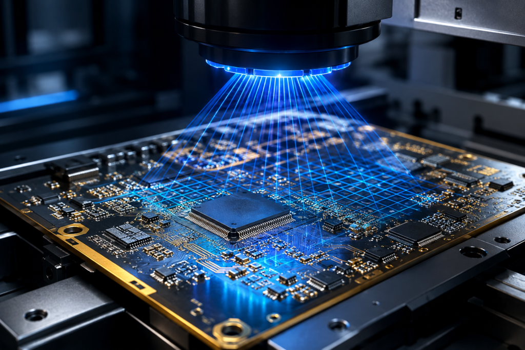
Scaling complex hardware from prototype to volume production fails when high-speed SMT lines lack real-time feedback loops. As components shrink to 0201 passives and 0.35mm pitch BGAs, achieving zero-defect New Product Introduction (NPI) requires replacing traditional visual checks with an integrated 3D inspection stack. The High-Precision NPI Challenge Modern power electronics and high-density designs leave no margin for process variance. Traditional NPI workflows rely heavily on post-reflow inspection, where defects like bridging, tombstoning, or head-in-pillow (HiP) are caught only after hundreds of boards have traversed the reflow oven. Reworking fine-pitch micro-BGAs or 01005 passives damages board substrates, compromises thermal integrity, and creates severe NPI delays. Eliminating rework loops during initial production runs demands catching process deviations at the exact moment they occur. The 3D Inspection Stack Achieving zero-defect SMT assembly relies on a continuous, multi-layer 3D inspection stack that validates solder geometry and joint formation across every stage of the line: Closed-Loop Process Optimization Data from the inspection stack is only as useful as the line’s ability to act on it. Modern high-precision SMT lines connect 3D SPI and 3D AOI machines directly back to the stencil printer and pick-and-place equipment in a closed feedback loop. When SPI detects a minor trend in paste offset, it automatically adjusts printer alignment and triggers stencil cleaning cycles before defects occur. Combined with rigorous Front-End Design for Manufacturability (DFM) analysis, closed-loop automation turns NPI from an unpredictable trial-and-error phase into a repeatable science. At Chipmates.in, we combine closed-loop SMT lines, advanced 3D inspection, and deep DFM engineering to take high-density designs from prototype to zero-defect mass production. Contact us today to review your NPI requirements and optimize your next hardware build.
Mastering India’s ₹40,000 Cr ECMS & Domestic Value Addition Rules: A Chennai Corridor Playbook
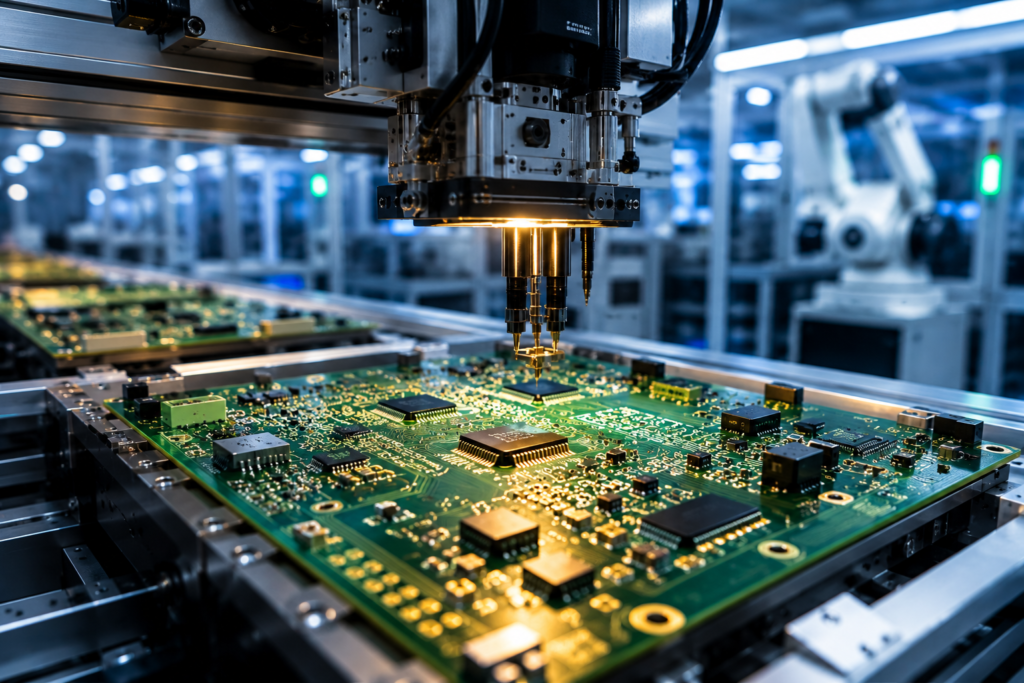
The Union Budget 2026-27 decision to boost the Electronics Components Manufacturing Scheme (ECMS) outlay to ₹40,000 crore forces a hard pivot for OEMs operating in India. Relying on basic box-build assembly is no longer enough; accessing government incentives now requires aggressive, deep component localization. The ₹40,000 Cr ECMS Shift The expanded ₹40,000 crore ECMS structure mandates a complete re-evaluation of OEM supply chains. To capture these capital and turnover-linked incentives, electronics manufacturers must pivot their focus toward localizing sub-assemblies and bare components. Scaling DVA (Domestic Value Addition) India’s current Domestic Value Addition (DVA) in electronics hovers around 18-20%. To qualify for tier-one fiscal incentives, OEMs must aggressively push those numbers upward without compromising global quality standards. The Chennai Corridor Advantage Executing this localization playbook requires the right structural foundation, making the Chennai/Sriperumbudur EMS cluster a highly strategic base of operations. This region provides the physical and intellectual resources necessary to scale DVA quickly and reliably. The Chipmates Advantage At Chipmates.in, we serve as the premier localized EMS partner in the Chennai corridor, directly enabling OEMs to achieve aggressive DVA compliance, source local components reliably, and maintain zero-defect manufacturing. Contact our team today to build a tactical, incentive-aligned localization strategy for your next production run.