
IPC Class 3 & Beyond: The ‘No-Fail’ Mandate for India’s Defense Electronics
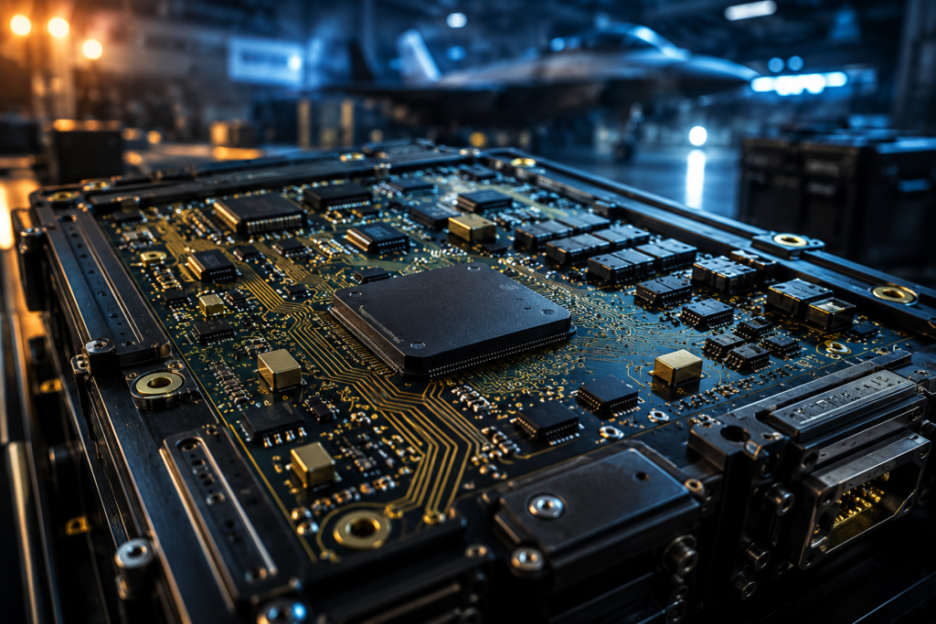
Imagine a tactical UAV (Unmanned Aerial Vehicle) banking sharply over the salt pans of the Thar Desert. The ambient temperature is hitting 48°C, and the internal housing of the motor controller is significantly hotter. Simultaneously, a loitering munition is deployed in the sub-zero, oxygen-thin atmosphere of Siachen. In both scenarios, the onboard electronics are subjected to violent vibrations, extreme thermal cycling, and G-forces that would shatter standard consumer hardware. If a smartphone reboots in your pocket, it’s an inconvenience. If a missile guidance system reboots during a terminal engagement, or a Battery Management System (BMS) fails in a stealth submarine, it is a national security catastrophe. In the theater of defense, there is no “Ctrl+Alt+Del.” There is only mission success or mission failure. As India accelerates its Atmanirbhar Bharat mandate through the latest Defense Acquisition Procedure (DAP), the focus is shifting from simply “Make in India” to “Reliably Build in India.” For the engineers and decision-makers at Chipmates, this is where the conversation begins and ends: IPC Class 3. Section 1: The Spectrum of Reliability In the Electronic Manufacturing Services (EMS) world, the IPC (Association Connecting Electronics Industries) standards define the quality and reliability of a Printed Circuit Board Assembly (PCBA). To understand defense electronics, one must understand these tiers: Class 3 requires more stringent inspections, higher solder joint volume, and tighter tolerances. It is the difference between a board that works in a lab and a board that survives a battlefield. Section 2: Why Consumer EMS Fails the Defense Sector India has seen a surge in “Mega-Factories” capable of churning out millions of consumer devices. While impressive, these facilities are fundamentally unsuited for defense electronics. Consumer EMS is built on the pillars of Speed and Cost-Down. Lines are optimized for high-volume, low-complexity runs where a 1% failure rate is an acceptable statistical noise. Defense electronics require an HMLV (High-Mix, Medium-Volume) approach. The production runs are smaller, the components are more specialized, and the engineering complexity is exponentially higher. A factory optimized for mobile phones cannot suddenly pivot to the slow, methodical, and hyper-documented precision required for MIL-SPEC (Military Specification) hardware. The culture of “fast and cheap” is the antithesis of “precise and permanent.” Section 3: The Three Pillars of Defense Manufacturing At our Greenfield facility in Chennai, we have built our SMT (Surface Mount Technology) lines to support three critical pillars of defense reliability: Pillar 1: Thermal Management Power electronics in defense systems—such as motor controllers for electric heavy-mobility vehicles—generate immense heat. Chipmates utilizes advanced DfM (Design for Manufacturing) protocols to ensure optimal heat dissipation. From specialized thermal interface materials to the precision placement of heavy-copper PCBs, we ensure the hardware maintains its integrity across a -55°C to +125°C range. Pillar 2: Mechanical Integrity Vibration is the silent killer of defense electronics. A cold solder joint that passes a standard functional test will fail after ten minutes of high-frequency vibration on a naval vessel. Our IPC Class 3 soldering protocols ensure maximum barrel fill and annular ring integrity. We utilize high-precision AOI (Automated Optical Inspection) and 3D X-Ray to verify the internal structure of BGA (Ball Grid Array) joints that the human eye cannot see. Pillar 3: Traceability and Anti-Counterfeit In defense, knowing the “pedigree” of a component is as important as its performance. Counterfeit semiconductors are a major threat to national security. Chipmates maintains a rigorous supply chain lock, ensuring full traceability from the silicon wafer to the final PCBA. We don’t just build the board; we provide the data trail that proves every capacitor and IC is genuine and verified. Section 4: The Strategic Chennai Hub for NPI Speed of innovation is now a tactical advantage. Located in the Redhills/Sriperumbudur corridor, Chipmates is positioned at the heart of India’s most robust industrial ecosystem. This proximity allows for rapid NPI (New Product Introduction). For defense PSUs and private aerospace contractors, the ability to iterate a design, run a medium-volume batch, and subject it to environmental stress testing (ESS) in the same hub is invaluable. We act as the “Special Ops” manufacturing partner for developers who need to move from prototype to battle-ready hardware without the bureaucratic inertia of mega-factories. Conclusion: No Second Chances As India’s defense sector transitions from being a global importer to a global exporter of high-tech systems, the manufacturing backbone must be irreproachable. A guidance system, a communication link, or a power unit is only as strong as its weakest solder joint. At Chipmates, we believe that “Made in India” must be synonymous with “World-Class Reliability.” We don’t just assemble boards; we engineer “Anti-Fragile” systems designed to perform when the stakes are at their highest. In the field, there is no second chance. Partner with a manufacturer that treats your mission as its own. Build for the No-Fail Mandate. Build with Chipmates.
Inside the Modern SMT Line: 3D Inspection, Zero-Defect NPI, and the Science of High-Precision Hardware

Scaling complex hardware from prototype to volume production fails when high-speed SMT lines lack real-time feedback loops. As components shrink to 0201 passives and 0.35mm pitch BGAs, achieving zero-defect New Product Introduction (NPI) requires replacing traditional visual checks with an integrated 3D inspection stack. The High-Precision NPI Challenge Modern power electronics and high-density designs leave no margin for process variance. Traditional NPI workflows rely heavily on post-reflow inspection, where defects like bridging, tombstoning, or head-in-pillow (HiP) are caught only after hundreds of boards have traversed the reflow oven. Reworking fine-pitch micro-BGAs or 01005 passives damages board substrates, compromises thermal integrity, and creates severe NPI delays. Eliminating rework loops during initial production runs demands catching process deviations at the exact moment they occur. The 3D Inspection Stack Achieving zero-defect SMT assembly relies on a continuous, multi-layer 3D inspection stack that validates solder geometry and joint formation across every stage of the line: Closed-Loop Process Optimization Data from the inspection stack is only as useful as the line’s ability to act on it. Modern high-precision SMT lines connect 3D SPI and 3D AOI machines directly back to the stencil printer and pick-and-place equipment in a closed feedback loop. When SPI detects a minor trend in paste offset, it automatically adjusts printer alignment and triggers stencil cleaning cycles before defects occur. Combined with rigorous Front-End Design for Manufacturability (DFM) analysis, closed-loop automation turns NPI from an unpredictable trial-and-error phase into a repeatable science. At Chipmates.in, we combine closed-loop SMT lines, advanced 3D inspection, and deep DFM engineering to take high-density designs from prototype to zero-defect mass production. Contact us today to review your NPI requirements and optimize your next hardware build.