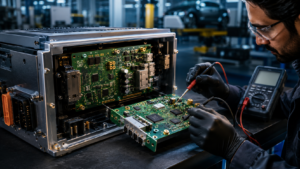
The push toward 800V+ EV powertrains, 1,500V solar central inverters, and utility-scale battery energy storage systems (BESS) is pushing power density to its physical limits. Designing for 1,000V DC and above is not simply an exercise in scaling up 400V topologies. Higher voltages drastically compress dielectric margins, generate severe thermal concentrations during fast switching cycles, and turn minor manufacturing anomalies into critical insulation failures.
Achieving long-term field reliability under these conditions requires aligning high-voltage thermal design with IPC Class 3 manufacturing discipline.
Thermal Management at High Voltage and Power Density
Switching topologies using Silicon Carbide (SiC) and Gallium Nitride (GaN) drastically shrink magnetic components and enable high switching frequencies, but they concentrate thermal output in smaller surface areas. Managing this heat without compromising electrical insulation demands multi-layered thermal strategies:
- Heavy Copper and Metal Core PCBs (MCPCBs): Heavy copper layers (3 oz to 10+ oz) handle localized high current densities, while MCPCBs or Direct Bonded Copper (DBC) ceramic substrates provide high dielectric strength coupled with low thermal resistance ($R_{th}$).
- Thermal Via Arrays: High-density, copper-filled, and flat-capped thermal vias under power MOSFETs efficiently sink heat away from junction points to inner copper planes.
- Encapsulation & Conformal Coatings: High-performance thermal potting compounds serve dual roles: transferring heat away from hot spots while reinforcing insulation resistance against moisture and environmental contaminants.
Dielectric Isolation: Creepage, Clearance, and CTI
High-voltage layouts fail primarily through dielectric breakdown or electrical tracking across board surfaces. Design and manufacturing must rigorously address spacing and substrate behavior under electrical stress:
- IPC-2221 Compliance: Clearance (air isolation) and creepage (surface distance) rules must account for altitude, working voltage, and worst-case transient overvoltages.
- High-CTI Laminates: Utilizing substrate materials with a high Comparative Tracking Index (CTI $\ge 600$) prevents carbon tracking and catastrophic dielectric breakdown over extended field operations.
- Milling Isolation Slots: Machining physical air slots between high-voltage nodes effectively interrupts creepage paths without expanding overall board dimensions.
IPC Class 3 Precision for Zero-Defect Assembly
At 1,000V+, standard IPC Class 2 assembly is insufficient. Minor solder voids or misaligned components become high-stress electric field concentrators. IPC Class 3 standards ensure continuous operation in harsh clean-tech environments:
| Process Parameter | IPC Class 2 Requirement | IPC Class 3 High-Voltage Requirement |
| Plated Through-Hole (PTH) Fill | 50% vertical fill | 75% minimum vertical fill for structural and electrical integrity |
| Annular Ring Tolerance | Breaks allowed up to 90° | Zero breakout permitted; minimum 2 mil annular ring edge space |
| Plating Thickness | Standard copper wrap | Heavy copper wrap plating to prevent micro-cracking under thermal cycling |
| Inspection Standards | Visual / 2D AOI sampling | 3D SPI/AOI + 100% X-ray inspection for void detection beneath power devices |
Proper solder joint volume and voiding limits ($\le 10-15\%$ directly under thermal pads) are critical. Voids distort current flow, create hot spots, and degrade the assembly’s thermal impedance over time.
At Chipmates, we bridge the gap between high-voltage power engineering and high-reliability EMS execution. From thermal DFM analysis and high-CTI substrate sourcing to IPC Class 3 SMT assembly and rigorous automated X-ray inspection, we build hardware meant to withstand extreme electrical and thermal stress.
Planning your next 1,000V+ power conversion project? Contact Chipmates.in today to review your DFM requirements.