
Engineering for 1,000V+: Thermal Management and IPC Class 3 Assembly Standards in Modern Clean-Tech Electronics
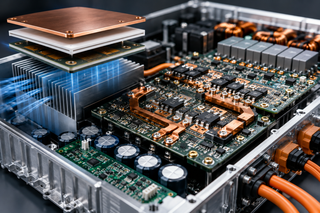
The push toward 800V+ EV powertrains, 1,500V solar central inverters, and utility-scale battery energy storage systems (BESS) is pushing power density to its physical limits. Designing for 1,000V DC and above is not simply an exercise in scaling up 400V topologies. Higher voltages drastically compress dielectric margins, generate severe thermal concentrations during fast switching cycles, and turn minor manufacturing anomalies into critical insulation failures. Achieving long-term field reliability under these conditions requires aligning high-voltage thermal design with IPC Class 3 manufacturing discipline. Thermal Management at High Voltage and Power Density Switching topologies using Silicon Carbide (SiC) and Gallium Nitride (GaN) drastically shrink magnetic components and enable high switching frequencies, but they concentrate thermal output in smaller surface areas. Managing this heat without compromising electrical insulation demands multi-layered thermal strategies: Dielectric Isolation: Creepage, Clearance, and CTI High-voltage layouts fail primarily through dielectric breakdown or electrical tracking across board surfaces. Design and manufacturing must rigorously address spacing and substrate behavior under electrical stress: IPC Class 3 Precision for Zero-Defect Assembly At 1,000V+, standard IPC Class 2 assembly is insufficient. Minor solder voids or misaligned components become high-stress electric field concentrators. IPC Class 3 standards ensure continuous operation in harsh clean-tech environments: Process Parameter IPC Class 2 Requirement IPC Class 3 High-Voltage Requirement Plated Through-Hole (PTH) Fill 50% vertical fill 75% minimum vertical fill for structural and electrical integrity Annular Ring Tolerance Breaks allowed up to 90° Zero breakout permitted; minimum 2 mil annular ring edge space Plating Thickness Standard copper wrap Heavy copper wrap plating to prevent micro-cracking under thermal cycling Inspection Standards Visual / 2D AOI sampling 3D SPI/AOI + 100% X-ray inspection for void detection beneath power devices Proper solder joint volume and voiding limits ($\le 10-15\%$ directly under thermal pads) are critical. Voids distort current flow, create hot spots, and degrade the assembly’s thermal impedance over time. At Chipmates, we bridge the gap between high-voltage power engineering and high-reliability EMS execution. From thermal DFM analysis and high-CTI substrate sourcing to IPC Class 3 SMT assembly and rigorous automated X-ray inspection, we build hardware meant to withstand extreme electrical and thermal stress. Planning your next 1,000V+ power conversion project? Contact Chipmates.in today to review your DFM requirements.
Designing Electronics for Field Serviceability
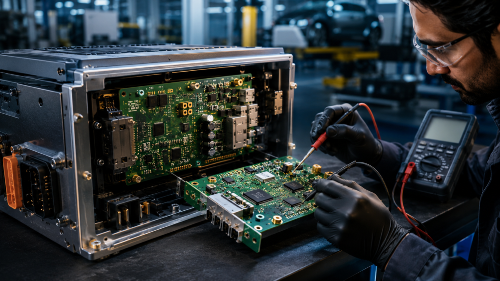
The real test of an electronic product may come years after it leaves the factory—when it fails in the field. A product can work perfectly in the laboratory and be manufactured consistently, yet still become difficult and expensive to maintain once it is deployed. For electronics used in vehicles, industrial environments, remote locations and defence applications, serviceability should be considered during engineering—not after a failure occurs. Why Serviceability Starts in Design Serviceability begins with decisions made long before production. How easily can a technician identify a failed board? Are diagnostic or test points accessible? Can a faulty module be replaced without replacing the entire assembly? Can the firmware version and board revision be identified quickly? These questions may not matter during a prototype demonstration. They matter considerably when a product is installed hundreds of kilometres away from the factory. A service-friendly design makes diagnosis and replacement part of the product architecture rather than an afterthought. What Makes Electronics Easier to Service? Consider an industrial controller that stops working at a remote customer site. Without clear diagnostics, the technician may not know whether the problem is in the power section, PCB, firmware or connected module. The safest option may appear to be removing the complete unit and sending it back to the manufacturer. A more serviceable design could provide accessible test points, clear fault information, identifiable PCB assemblies and replaceable modules. The technician can isolate the problem, replace the affected assembly and restore operation without unnecessary factory return. The difference is not simply convenience. It can mean less downtime, lower logistics costs and faster recovery. The same principle applies to EV electronics, Industrial IoT equipment, surveillance systems and defence electronics, where equipment may be deployed in environments where immediate factory support is not practical. The Cost of Poor Serviceability Poor serviceability often creates costs that are invisible during product development. When fault diagnosis is difficult, service teams may replace complete units rather than individual assemblies. Warranty returns increase. Engineers spend more time investigating field failures. Replacement logistics become more complicated. Over time, these costs can outweigh the small additional effort required during the original design phase. Serviceability therefore belongs alongside manufacturability, reliability and testability when evaluating an electronic product. Field Failures Should Improve the Next Revision Serviceability is also about learning from what happens after deployment. When a failed board can be identified through serialisation, revision history, firmware records and manufacturing traceability, engineers have better information for investigating the problem. That creates a useful feedback loop: Design → Manufacturing → Testing → Field Deployment → Failure Analysis → Design Improvement Instead of treating a field failure as an isolated event, it becomes input for the next product revision. The Chipmates Perspective At Chipmates, we see electronics manufacturing as part of a wider product lifecycle. For high-reliability electronics, testability, diagnostics, traceability, modularity and controlled revisions should work together to make products easier to understand and maintain after they leave the factory. An EMS partner should think beyond the production line and consider what happens when the board is in the field, under real operating conditions. Good electronics design does not stop at making the product work. It considers how that product will be diagnosed, repaired and supported when it matters most.