
IPC Class 3 & Beyond: The ‘No-Fail’ Mandate for India’s Defense Electronics
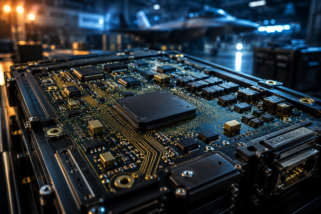
Imagine a tactical UAV (Unmanned Aerial Vehicle) banking sharply over the salt pans of the Thar Desert. The ambient temperature is hitting 48°C, and the internal housing of the motor controller is significantly hotter. Simultaneously, a loitering munition is deployed in the sub-zero, oxygen-thin atmosphere of Siachen. In both scenarios, the onboard electronics are subjected to violent vibrations, extreme thermal cycling, and G-forces that would shatter standard consumer hardware. If a smartphone reboots in your pocket, it’s an inconvenience. If a missile guidance system reboots during a terminal engagement, or a Battery Management System (BMS) fails in a stealth submarine, it is a national security catastrophe. In the theater of defense, there is no “Ctrl+Alt+Del.” There is only mission success or mission failure. As India accelerates its Atmanirbhar Bharat mandate through the latest Defense Acquisition Procedure (DAP), the focus is shifting from simply “Make in India” to “Reliably Build in India.” For the engineers and decision-makers at Chipmates, this is where the conversation begins and ends: IPC Class 3. Section 1: The Spectrum of Reliability In the Electronic Manufacturing Services (EMS) world, the IPC (Association Connecting Electronics Industries) standards define the quality and reliability of a Printed Circuit Board Assembly (PCBA). To understand defense electronics, one must understand these tiers: Class 3 requires more stringent inspections, higher solder joint volume, and tighter tolerances. It is the difference between a board that works in a lab and a board that survives a battlefield. Section 2: Why Consumer EMS Fails the Defense Sector India has seen a surge in “Mega-Factories” capable of churning out millions of consumer devices. While impressive, these facilities are fundamentally unsuited for defense electronics. Consumer EMS is built on the pillars of Speed and Cost-Down. Lines are optimized for high-volume, low-complexity runs where a 1% failure rate is an acceptable statistical noise. Defense electronics require an HMLV (High-Mix, Medium-Volume) approach. The production runs are smaller, the components are more specialized, and the engineering complexity is exponentially higher. A factory optimized for mobile phones cannot suddenly pivot to the slow, methodical, and hyper-documented precision required for MIL-SPEC (Military Specification) hardware. The culture of “fast and cheap” is the antithesis of “precise and permanent.” Section 3: The Three Pillars of Defense Manufacturing At our Greenfield facility in Chennai, we have built our SMT (Surface Mount Technology) lines to support three critical pillars of defense reliability: Pillar 1: Thermal Management Power electronics in defense systems—such as motor controllers for electric heavy-mobility vehicles—generate immense heat. Chipmates utilizes advanced DfM (Design for Manufacturing) protocols to ensure optimal heat dissipation. From specialized thermal interface materials to the precision placement of heavy-copper PCBs, we ensure the hardware maintains its integrity across a -55°C to +125°C range. Pillar 2: Mechanical Integrity Vibration is the silent killer of defense electronics. A cold solder joint that passes a standard functional test will fail after ten minutes of high-frequency vibration on a naval vessel. Our IPC Class 3 soldering protocols ensure maximum barrel fill and annular ring integrity. We utilize high-precision AOI (Automated Optical Inspection) and 3D X-Ray to verify the internal structure of BGA (Ball Grid Array) joints that the human eye cannot see. Pillar 3: Traceability and Anti-Counterfeit In defense, knowing the “pedigree” of a component is as important as its performance. Counterfeit semiconductors are a major threat to national security. Chipmates maintains a rigorous supply chain lock, ensuring full traceability from the silicon wafer to the final PCBA. We don’t just build the board; we provide the data trail that proves every capacitor and IC is genuine and verified. Section 4: The Strategic Chennai Hub for NPI Speed of innovation is now a tactical advantage. Located in the Redhills/Sriperumbudur corridor, Chipmates is positioned at the heart of India’s most robust industrial ecosystem. This proximity allows for rapid NPI (New Product Introduction). For defense PSUs and private aerospace contractors, the ability to iterate a design, run a medium-volume batch, and subject it to environmental stress testing (ESS) in the same hub is invaluable. We act as the “Special Ops” manufacturing partner for developers who need to move from prototype to battle-ready hardware without the bureaucratic inertia of mega-factories. Conclusion: No Second Chances As India’s defense sector transitions from being a global importer to a global exporter of high-tech systems, the manufacturing backbone must be irreproachable. A guidance system, a communication link, or a power unit is only as strong as its weakest solder joint. At Chipmates, we believe that “Made in India” must be synonymous with “World-Class Reliability.” We don’t just assemble boards; we engineer “Anti-Fragile” systems designed to perform when the stakes are at their highest. In the field, there is no second chance. Partner with a manufacturer that treats your mission as its own. Build for the No-Fail Mandate. Build with Chipmates.
Inside the Modern SMT Line: 3D Inspection, Zero-Defect NPI, and the Science of High-Precision Hardware
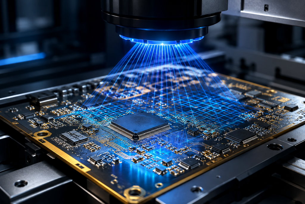
Scaling complex hardware from prototype to volume production fails when high-speed SMT lines lack real-time feedback loops. As components shrink to 0201 passives and 0.35mm pitch BGAs, achieving zero-defect New Product Introduction (NPI) requires replacing traditional visual checks with an integrated 3D inspection stack. The High-Precision NPI Challenge Modern power electronics and high-density designs leave no margin for process variance. Traditional NPI workflows rely heavily on post-reflow inspection, where defects like bridging, tombstoning, or head-in-pillow (HiP) are caught only after hundreds of boards have traversed the reflow oven. Reworking fine-pitch micro-BGAs or 01005 passives damages board substrates, compromises thermal integrity, and creates severe NPI delays. Eliminating rework loops during initial production runs demands catching process deviations at the exact moment they occur. The 3D Inspection Stack Achieving zero-defect SMT assembly relies on a continuous, multi-layer 3D inspection stack that validates solder geometry and joint formation across every stage of the line: Closed-Loop Process Optimization Data from the inspection stack is only as useful as the line’s ability to act on it. Modern high-precision SMT lines connect 3D SPI and 3D AOI machines directly back to the stencil printer and pick-and-place equipment in a closed feedback loop. When SPI detects a minor trend in paste offset, it automatically adjusts printer alignment and triggers stencil cleaning cycles before defects occur. Combined with rigorous Front-End Design for Manufacturability (DFM) analysis, closed-loop automation turns NPI from an unpredictable trial-and-error phase into a repeatable science. At Chipmates.in, we combine closed-loop SMT lines, advanced 3D inspection, and deep DFM engineering to take high-density designs from prototype to zero-defect mass production. Contact us today to review your NPI requirements and optimize your next hardware build.
Mastering India’s ₹40,000 Cr ECMS & Domestic Value Addition Rules: A Chennai Corridor Playbook
The Union Budget 2026-27 decision to boost the Electronics Components Manufacturing Scheme (ECMS) outlay to ₹40,000 crore forces a hard pivot for OEMs operating in India. Relying on basic box-build assembly is no longer enough; accessing government incentives now requires aggressive, deep component localization. The ₹40,000 Cr ECMS Shift The expanded ₹40,000 crore ECMS structure mandates a complete re-evaluation of OEM supply chains. To capture these capital and turnover-linked incentives, electronics manufacturers must pivot their focus toward localizing sub-assemblies and bare components. Scaling DVA (Domestic Value Addition) India’s current Domestic Value Addition (DVA) in electronics hovers around 18-20%. To qualify for tier-one fiscal incentives, OEMs must aggressively push those numbers upward without compromising global quality standards. The Chennai Corridor Advantage Executing this localization playbook requires the right structural foundation, making the Chennai/Sriperumbudur EMS cluster a highly strategic base of operations. This region provides the physical and intellectual resources necessary to scale DVA quickly and reliably. The Chipmates Advantage At Chipmates.in, we serve as the premier localized EMS partner in the Chennai corridor, directly enabling OEMs to achieve aggressive DVA compliance, source local components reliably, and maintain zero-defect manufacturing. Contact our team today to build a tactical, incentive-aligned localization strategy for your next production run.
From Pure EMS to Joint-ODM: Decoupling Indian Hardware from Foreign IP Dependencies
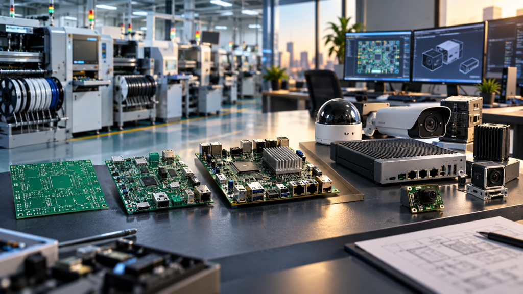
A product can be manufactured in India without the technology behind it being Indian. A PCB may be assembled locally, tested locally and shipped from an Indian factory, while its processor, reference design, firmware ecosystem and core intellectual property remain controlled elsewhere. That distinction is becoming increasingly important as India moves from electronics assembly toward deeper product and technology ownership. The Limitation of the Pure EMS Model In a traditional EMS (Electronics Manufacturing Services) relationship, the OEM owns the design and the EMS provider manufactures it. This model works well when the primary requirement is production capacity. But as products become more complex, manufacturing and engineering can no longer operate completely separately. If the manufacturer is involved only after the design is finalised, opportunities to improve architecture, manufacturability, component strategy and product scalability may be limited. The result can be a product that is successfully manufactured in India, but whose critical technology remains dependent on external platforms. This is not necessarily a weakness. Modern electronics will continue to rely on global components and technologies. The strategic question is how much of the product knowledge, architecture and IP can be developed and controlled within India. Why Joint-ODM Changes the Equation The next step is not simply moving from EMS to ODM. A Joint-ODM model creates a collaborative relationship between the OEM and manufacturing partner. Instead of: “Here is my design. Please build it.” the conversation becomes: “Let us build and evolve the product together.” The manufacturing partner can contribute to hardware architecture, DFM, product engineering, testing and production optimisation, while the OEM retains clearly defined ownership of its strategic IP. This can shorten the distance between engineering and manufacturing, reduce avoidable redesigns and create reusable hardware platforms for future products. For an Indian hardware company, that capability can be significant. The objective is not to eliminate foreign technology overnight, but to progressively reduce unnecessary dependency. Why Indian IP Matters Global technology competition, supply-chain diversification and tighter controls around strategic technologies have made technology ownership a business consideration—not just an engineering one. This matters particularly in defence, surveillance, EV and Industrial IoT. Consider an Indian company developing an intelligent surveillance product. Under a pure EMS model, the company supplies the completed design and the manufacturer builds it. Under a Joint-ODM model, the manufacturing partner can participate earlier in hardware architecture, production engineering and product-platform development. That platform may then support multiple product variants. The relationship moves from manufacturing a product to helping develop a product family. The Opportunity for Indian Electronics India does not need to build every semiconductor, component or software platform domestically to become more technologically capable. A more practical path is to increase ownership of the layers that differentiate the product: system architecture, hardware design, firmware, integration, product engineering and application-specific IP. That is where the transition from “assembled in India” toward “designed, developed and manufactured in India” becomes meaningful. It is also where a capable EMS company can evolve into a technology-development partner without competing directly with its OEM customers. The Chipmates Perspective At Chipmates, we see the future of Indian EMS extending beyond contract manufacturing. Our direction toward Joint-ODM and product co-development, including work on proprietary AI-enabled CCTV/DVR hardware, reflects a broader belief: manufacturing capability should increasingly connect with engineering and product innovation. The goal is not complete technological isolation. It is greater control over the technology that creates product differentiation and long-term value. India’s electronics journey should not stop at making more products. The bigger opportunity is to build products whose engineering, innovation and intellectual property increasingly originate in India.
Engineering for 1,000V+: Thermal Management and IPC Class 3 Assembly Standards in Modern Clean-Tech Electronics
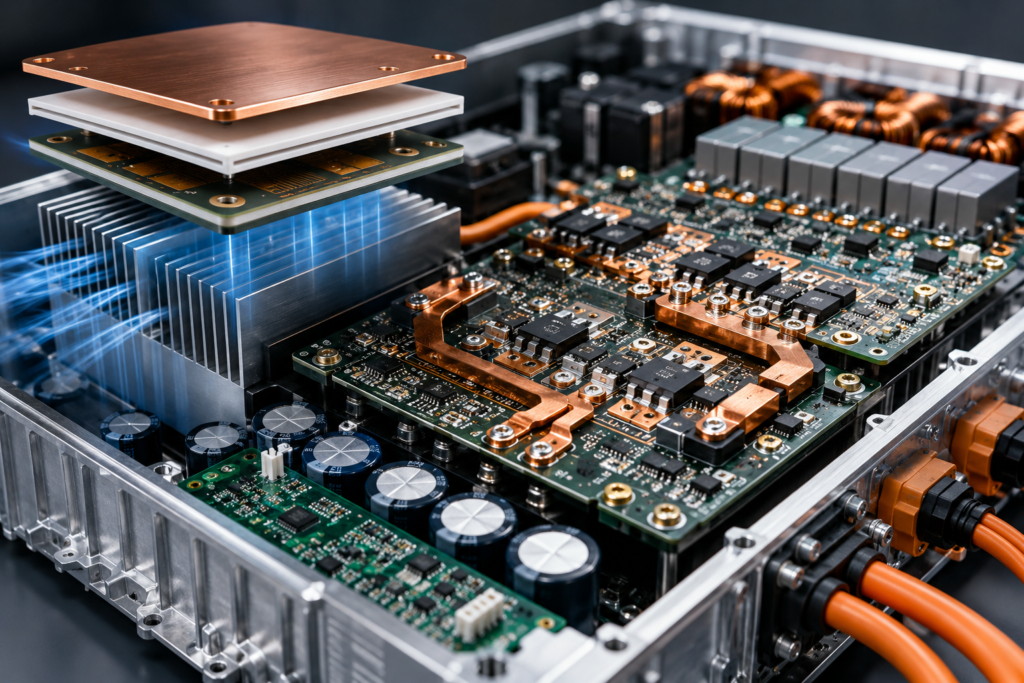
The push toward 800V+ EV powertrains, 1,500V solar central inverters, and utility-scale battery energy storage systems (BESS) is pushing power density to its physical limits. Designing for 1,000V DC and above is not simply an exercise in scaling up 400V topologies. Higher voltages drastically compress dielectric margins, generate severe thermal concentrations during fast switching cycles, and turn minor manufacturing anomalies into critical insulation failures. Achieving long-term field reliability under these conditions requires aligning high-voltage thermal design with IPC Class 3 manufacturing discipline. Thermal Management at High Voltage and Power Density Switching topologies using Silicon Carbide (SiC) and Gallium Nitride (GaN) drastically shrink magnetic components and enable high switching frequencies, but they concentrate thermal output in smaller surface areas. Managing this heat without compromising electrical insulation demands multi-layered thermal strategies: Dielectric Isolation: Creepage, Clearance, and CTI High-voltage layouts fail primarily through dielectric breakdown or electrical tracking across board surfaces. Design and manufacturing must rigorously address spacing and substrate behavior under electrical stress: IPC Class 3 Precision for Zero-Defect Assembly At 1,000V+, standard IPC Class 2 assembly is insufficient. Minor solder voids or misaligned components become high-stress electric field concentrators. IPC Class 3 standards ensure continuous operation in harsh clean-tech environments: Process Parameter IPC Class 2 Requirement IPC Class 3 High-Voltage Requirement Plated Through-Hole (PTH) Fill 50% vertical fill 75% minimum vertical fill for structural and electrical integrity Annular Ring Tolerance Breaks allowed up to 90° Zero breakout permitted; minimum 2 mil annular ring edge space Plating Thickness Standard copper wrap Heavy copper wrap plating to prevent micro-cracking under thermal cycling Inspection Standards Visual / 2D AOI sampling 3D SPI/AOI + 100% X-ray inspection for void detection beneath power devices Proper solder joint volume and voiding limits ($\le 10-15\%$ directly under thermal pads) are critical. Voids distort current flow, create hot spots, and degrade the assembly’s thermal impedance over time. At Chipmates, we bridge the gap between high-voltage power engineering and high-reliability EMS execution. From thermal DFM analysis and high-CTI substrate sourcing to IPC Class 3 SMT assembly and rigorous automated X-ray inspection, we build hardware meant to withstand extreme electrical and thermal stress. Planning your next 1,000V+ power conversion project? Contact Chipmates.in today to review your DFM requirements.
Electronics Lifecycle Engineering: Designing Beyond the First Production Run
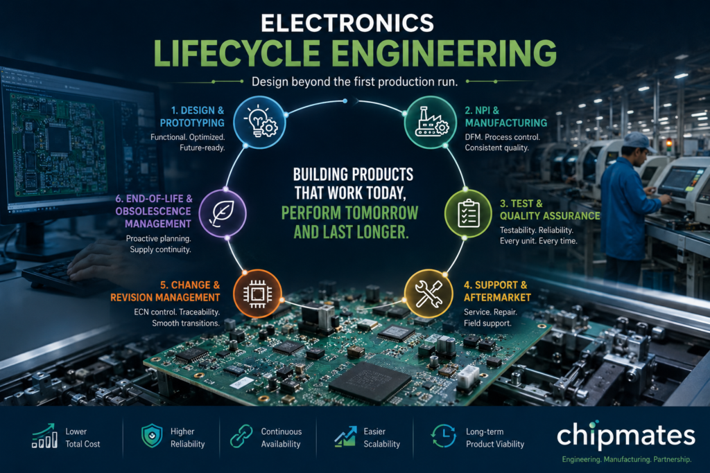
An electronics product is not finished when the prototype works. In many cases, that is when the harder questions begin. Can it be manufactured consistently? Will the components remain available? Can every unit be tested reliably? What happens when a component becomes obsolete or the product needs a revision two years later? These questions highlight the importance of Electronics Lifecycle Engineering—an approach that considers the product from initial design through manufacturing, support and eventual end-of-life. What Is Electronics Lifecycle Engineering? Electronics Lifecycle Engineering means looking at the complete journey of a product instead of treating manufacturing as the final stage. A design decision made during development can affect production cost, testability, sourcing, reliability and serviceability much later. Lifecycle engineering brings these considerations into the engineering process early, when changes are easier and less expensive to make. For OEMs and product companies, this creates a more practical connection between engineering intent and production reality. Where Lifecycle Challenges Appear The lifecycle begins with product design and prototyping. At this stage, the focus is usually on functionality and performance. But as the design moves into NPI and volume manufacturing, other factors become critical. A component that worked well in a prototype may have limited availability. A PCB may be difficult to assemble consistently at scale. Test access that was convenient during development may not be practical on a production line. Then comes change management. Component substitutions, firmware updates, PCB revisions and process changes must be controlled carefully. Without proper revision control and traceability, even a small engineering change can create production and quality issues. The lifecycle also continues after manufacturing. Repair, service, field support and component availability become increasingly important, particularly for products expected to remain in the market for several years. Eventually, component obsolescence becomes a reality. A lifecycle approach considers this early rather than waiting until a critical part disappears from the supply chain. Why Think Beyond Production? The cost of an electronics product is not determined only by its manufacturing price. Design choices influence assembly time, test requirements, component sourcing, rework, reliability and long-term service. Addressing these factors earlier can reduce avoidable engineering changes and production disruptions later. This is especially relevant for products where reliability and continuity are essential. The goal is not simply to manufacture a product successfully today, but to make sure it can continue to be manufactured and supported tomorrow. The Role of an EMS Partner A capable EMS partner can contribute much earlier than the production stage. Through Design for Manufacturing (DFM), component strategy, testability planning, process control and traceability, manufacturing considerations can become part of the product development conversation. This creates a stronger connection between design engineering, NPI and factory execution. It also gives OEMs a clearer path for managing revisions, scaling production and addressing lifecycle risks. At Chipmates, we see electronics manufacturing as part of a larger engineering lifecycle—not simply the final step after design. The real objective is straightforward: build products that are not only functional, but manufacturable, reliable, supportable and viable throughout their lifecycle. Because successful electronics engineering is not just about making a product work once. It is about making it work consistently, at scale, and for as long as the product needs to remain in the field.
The OEM–Factory Engineering Gap
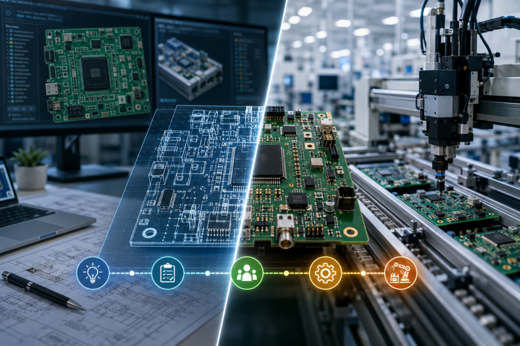
A prototype proving that something works does not prove that it is ready to manufacture. This is one of the most overlooked challenges in electronics product development. An OEM’s engineering team may validate the circuit, confirm functionality and build a successful prototype. But when that same design moves toward production, entirely different questions emerge: Can it be assembled consistently? Can every unit be tested? Are the components available? Can the design be scaled without introducing reliability problems? The gap between those questions is the OEM–Factory Engineering Gap. Where the Gap Begins OEM engineering teams are naturally focused on product performance, functionality and time-to-market. Manufacturing teams have a different responsibility: repeatability. A design that works once may not work efficiently thousands of times. A PCB, for example, may function perfectly in a prototype but create difficulties on the production line because of component placement, assembly orientation, limited test access or process constraints. Similarly, a component selected during development may later create sourcing challenges or require substitution. These issues are rarely caused by poor engineering. They often arise because design engineering and manufacturing engineering are solving different problems at different stages. What Gets Missed Before Production Many manufacturing challenges become visible only during NPI. A test point that was convenient during development may be difficult to access in production. Firmware that was manually loaded onto prototypes may require a controlled programming process. A carefully selected component may have limited availability. Tolerances that were acceptable in small batches may become a reliability concern when production volumes increase. Then there is documentation. Incomplete BOM information, unclear revisions or engineering changes can create confusion between the OEM, EMS partner and production team. By the time these problems surface, the cost of correction has already increased. The result can be additional iterations, delayed production, rework, engineering changes and avoidable NPI costs. Manufacturing Should Enter the Conversation Earlier The solution is not to make manufacturing responsible for product design. It is to make manufacturing part of the engineering conversation earlier. A strong EMS partnership should bring manufacturing perspectives into the product industrialisation process. Design for Manufacturing (DFM), testability, component availability, programming requirements, assembly constraints and traceability can then be considered before production begins. This is particularly important for EV electronics, Industrial IoT products and defence systems, where reliability and repeatability matter as much as getting the first prototype to work. The objective should be simple: Move manufacturing problems upstream, when they are still inexpensive to solve. From Engineering Intent to Production Reality At Chipmates, we see manufacturing as more than the final step after product development. The real challenge is translating engineering intent into repeatable production. That means asking practical questions early: Is the design manufacturable? Is it testable? Can it be produced consistently? Can revisions be controlled? Can the manufacturing history of each board be traced? This approach connects OEM engineering, NPI and factory execution rather than treating them as separate stages. The best manufacturing partner is not simply the one that receives a finished design and assembles it. It is the one that helps make the design production-ready before the factory has to pay the price for discovering what was missed.